Innovative Wafer Services for Modern Semiconductor Solutions
Have you ever wondered how small chips in our phones and computers can do so much with such tiny parts? Many people use these devices every day without knowing what makes them work so well. Modern chipmaking depends on advanced wafer work that keeps getting better each year.
These steps help companies build faster and more reliable parts for everyday tools. In this guide, you will learn how innovative wafer services shape the future of electronics. By the end, you will understand key steps, simple ideas, and the value behind modern semiconductor solutions.
How Wafer Services Shape Today’s Technology
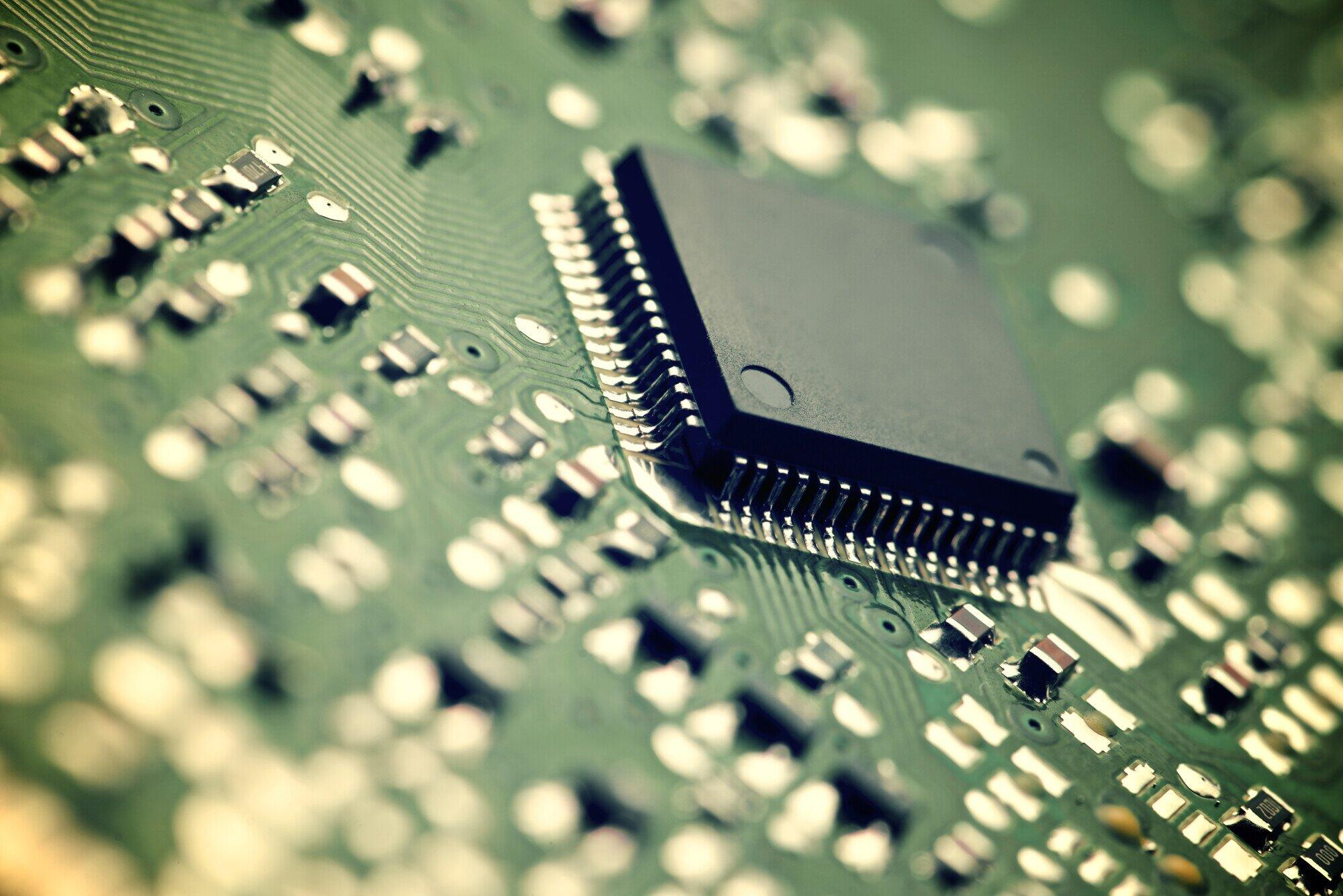
Wafer services sit at the center of many electronics we use each day. These services help shape, clean, prepare, and check the thin slices of material that hold tiny circuits.
When done with care, these steps improve how fast a device works and how long it lasts. Many companies rely on these processes because even a small mistake can cause big problems later.
Teams in this field use tools that form smooth and even surfaces. A clean and steady surface is important because it helps the circuits stick and work with fewer errors. Without strong wafer services, chips would not reach the quality needed for phones, laptops, cars, and many home devices.
Why Material Quality Matters In Modern Chipmaking
A good wafer starts with good materials. Companies often use silicon because it handles heat and power well.
Silicon also reacts in a steady and useful way when connected with other tiny parts. When the base material is strong, the rest of the chip can perform better and stay stable for a long time.
A high-quality wafer also creates fewer problems during the building process. With fewer weak spots, chips show better results and meet the needs of more devices.
This may sound simple, but it is one of the most important parts of the entire system. Many modern tools depend on the success of this early step.
Innovative Steps That Improve Wafer Performance
New methods help make the entire chipmaking process easier to control. One of these steps includes surface treatment that makes the wafer even and smooth.
Another step uses special cleaning tools to remove tiny particles that are too small to see. These cleaning steps help the wafer reach better accuracy when it moves to the next stage.
Some teams also use light-based tools to check the wafer without touching it. These checks help find tiny marks that may cause trouble later. With these tools, workers can see early signs of stress or uneven spots.
Fixing these issues early helps the wafer stay strong during the rest of the process. Many modern lines have added advanced coating steps too, making each layer bond better and last longer.
The Growing Need For Efficient Wafer Processing
As devices grow smaller, the need for precision grows even faster. A tiny change in size can affect the entire circuit. This is why companies depend on efficient wafer processing.
Smooth steps keep the parts steady and improve the power use of the chip. Good processing also helps the final tools stay cool when running for long periods.
Today’s designers want parts that do more while using less power. Efficient wafers allow this by supporting smaller and more complex layouts.
When the processing lines work well, designers can try new ideas without fear that the base material will fail. This supports faster research and easier upgrades to future products.
How New Tools Improve Modern Semiconductor Solutions
New tools play a big part in better wafer work. Many teams use machines that can measure tiny points with great accuracy. These machines help speed up tests and keep the results steady.
They also reduce guesswork during the building stage. Better tools mean better results and fewer delays.
Some tools can shape wafers with a very fine level of detail. These steps help companies build advanced layouts for new chips. This is where innovative wafer services show their full strength.
They help create strong support for circuits that may include millions of tiny parts. With these tools, the chip can stay reliable even when running hard tasks.
The Role Of Patterned Silicon In Advanced Devices
Inside many operations, a single phrase shows how advanced these processes have become. Many companies seek patterned silicon wafers because they improve testing and support advanced layouts.
They help teams study how new designs handle heat and power before moving to full production. This step is useful because it saves time, lowers risks, and helps experts build better models.
Why Cleanroom Control Supports Better Wafer Quality
A cleanroom is a space with very low dust and other small particles. Workers wear full suits to keep the air free from anything that may harm the wafer. Even a tiny dust spot could ruin the top layer of a wafer, so cleanrooms are very important.
These rooms use special air filters and steady airflow. The air moves in one direction and removes unwanted particles. This helps wafers stay clean during steps like coating, shaping, and measuring.
Cleanroom work is quiet, careful, and slow. Every small part of the wafer benefits from this level of care because it reduces errors that could affect the final chip.
How Wafer Testing Supports Long-Term Performance
Testing is one of the last steps in the wafer process. Workers check the wafer for signs of stress, heat trouble, or broken parts.
These tests help teams understand how well the wafer performed during earlier steps. They also help predict how the final chip will act when used in devices.
Some tests use light to scan the surface for defects. Other tests use small tools that apply gentle pressure.
When tests show strong results, companies feel more confident moving the wafer to the next stage. This helps build trust in the final product and supports better performance in consumer tools.
A Strong Closing Look At The Future Of Wafer Services
The world of electronics moves fast, and wafer services play a vital role in each step. These services shape the small slices of material that hold the heart of every modern device. As new devices grow smaller and smarter, strong wafer work will stay important.
You now have a clear look at how these steps support better performance, power savings, and long-term success. With this knowledge, you have a better understanding of how modern semiconductor solutions depend on careful and steady work.
Did this guide help you? Browse the rest of this section for more advice on a variety of topics.